The VC7xxx-series is a highly integrated wireless MCU which is a perfect fit to Wi-SUN and IoT applications.

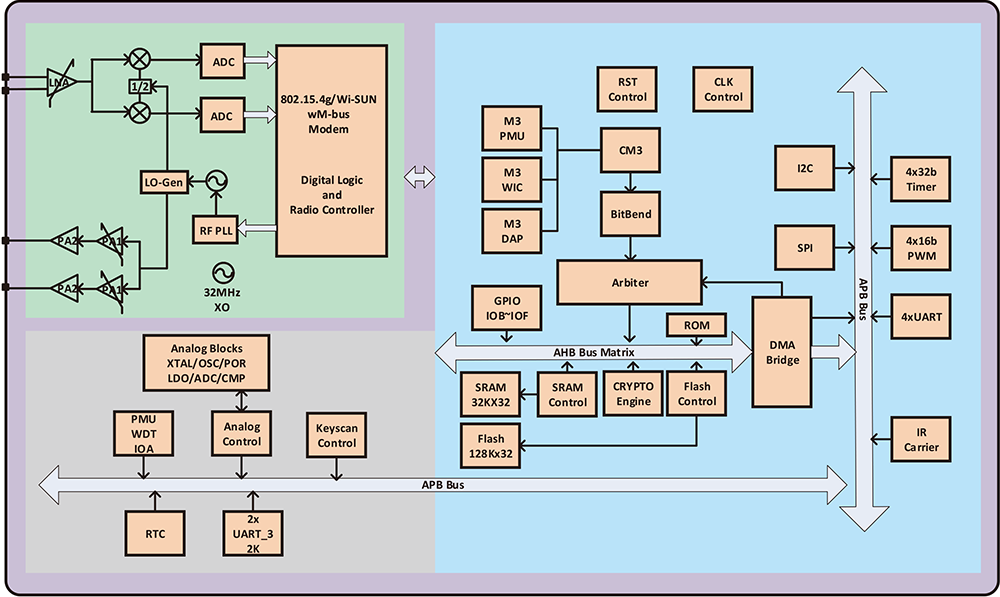
The VC7xxx-series is a highly-integrated wireless MCU designed for IoT applications. It integrates a Cortex-M3 MCU, a high-performance sub-1GHz radio, Flash and SRAM memory, various interfaces (e.g., UART, SPI, I2C, PWM) and functionalities such as ADC and high precision timer. VC7xxx-series also supports power saving modes for low-power usages. The embedded sub-1GHz wireless transceiver is fully compliant to IEEE802.15.4g/x. It integrates the high-perfomance LNA and PAs (13dBm or 20dBm) for low power consumption and long-range wireless links. The advanced DSP technology ensures that the VC73xx can provide the best communication system performance in its class, such as the maximum link budget, the high ACI rejection and more.
Specifically, VC7000 allows customers to add wireless link capability to MCUs of their own choices. Moreover, VC7200 provides advanced mesh networking capabilities and open-CPU for small-to-medium scale IoT applications, while VC7300 (compliant to Wi-SUN FAN1.0) and VC7351 (compliant to Wi-SUN FAN1.1) support large-scale industrial IoT applications such as smart metering.
Best-in-class sub-1GHz RF transceiver compliant to IEEE802.15.4g/x
ARM Cortex-M3 CPU with embedded flash and SRAM memory
Support large scale networking (Wi-SUN FAN 1.0 and FAN 1.1)
Support small-to-medium scale easy networking
Support real-time applications
Embedded hardware security accelerator
Abundant interfaces for versitile IoT appliations
Low power consumption
MCU
Interface Controller
Analog Controller
Support IEEE 802.15.4g/x, wireless M-Bus
Support modulation schemes: OOK, 4/(G)FSK, GMSK and OFDM
Support sub-1GHz bands: 230, 315, 433, 490, 868, 915 MHz
Excellent selectivity performance
Best-in-class receiver sensitivity
Maximum data rate: 300 kbps (FSK) and 3.6Mbps (OFDM)
Configurable maximum transmit output power :
Automatic output power ramping
Automatic RX wake-up for low power listen
Fast wake-up and AGC for low power listen
Functions for link robustness:
RSSI and clear channel assessment for listen-before-talk
Support packet over packet reception for reliable communication
Early reception termination:
Operating Voltage: 2.0 V ~ 3.6 V
Package:
Operation Temperature: -40 ~ +85 °C
Power consumption of VC7000:
Power consumption of SoCs:
| Part Number | Flash | RAM | Package | Body Size(mm) |
|---|---|---|---|---|
| VC7300AU | 512 KB | 128 KB | QFN-64 | 9x9 |
| VC7300BU | 1 MB | 128 KB | QFN-64 | 9x9 |
All Rights Reserved © 2024 VertexCom www.vertexcom.com